

Silicon photonics technology was hotly discussed during the SEMICON Taiwan 2023. At the Silicon Photonics Global Summit held September 5 alongside the exhibition, I was invited to join discussions with experts from TSMC, ASE, Industrial Technology Research Institute (ITRI), US-based Cisco Systems and Advantest of Japan, with ASE CEO Tien Wu serving as the moderator. Together, we delved into the role that Si photonics technology can play in the era of artificial intelligence (AI). The following are my views presented on this topic.
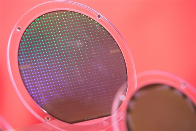
As widely known, Si photonics technology has undergone over 20 years of development. It primarily leverages mature CMOS (complementary metal-oxide-semiconductor) processes to integrate key active and passive optical components, such as waveguides, modulators, gratings, couplers and even photodetectors, onto silicon substrates for processing optical signals. The only component that cannot be integrated directly onto such substrates is semiconductor laser, as it involves a different material system and can be addressed only through packaging methods. In the silicon photonics platform, a silicon substrate is responsible for converting optical signals into electrical signals, serving as the receiving end. On the other hand, the transmitting end involves converting electrical signals into optical signals through lasers. Basically, utilizing mature semiconductor manufacturing processes boasts advantages in terms of miniaturization, integration, production yield and cost; and employing optical signals also offers advantages such as high bandwidth, low latency, and low power consumption when compared to electrical signals.
Since the introduction of optical fiber communication in the 1980s, it has played a crucial role in signal transmission. In its early days, when human data usage was relatively low, optical communication was mainly used for long-distance transmission, such as undersea cables and metropolitan networks. As data usage has increased, optical communication has also entered the realm of regional networks. With the recent rise of generative AI, the most substantial data generation and transmission occur between AI servers. This is because any large-scale model contains billions of parameters, and the computational power required for each training session is immense, all having to rely on parallel processing and data exchange between chips.
Thanks to semiconductor manufacturing technology advancements, it now takes only 1-2 nanoseconds to process or compute a single instruction. However, the increase in data transmission speed has never been able to keep up with the growth in computing power. Light traveling within an optical fiber incurs a delay of approximately five nanoseconds per meter. Consequently, AI servers often have to wait for data to be transmitted, leading to periods of inactivity; but if electrical signals were used, instead of optical signals, for transmission, the waiting time would be even longer. In this regard, the solution is, of course, to bring the devices responsible for converting optical signals closer to the CPU/GPU/ASIC chips to reduce signal latency, ideally avoiding the use of circuit boards in between. This is where co-package optics (CPO), including silicon photonics substrates, comes into play.
Currently, CPO is primarily being deployed inside switches. It involves stacking Si photonics substrates with ICs for processing electrical signals, which are then connected to optical fibers and put in close proximity to various IC processors, representing the closest and lowest-latency solution available.
In the mid-2000s, IBM, in its annual Technology Outlook, particularly highlighted optical interconnect as a key focus for future technology. At that time, no people could foresee the rapid development of AI computing, nor did they have a clear picture of semiconductor technology progressing to levels below 3nm. However, it's clear that human reliance on data transmission would keep increasing, with Si photonics technology to play a role in optical interconnect.
At the time when optical interconnect was introduced, it was unclear whether they would be used for connecting signals between chips (chip-to-chip), between boards (board-to-board), or between racks of servers (rack-to-rack). Today, optical interconnect technology is widely adopted for signal connections between server racks and even between layers within a rack (unit-to-unit). Meanwhile, signal connections between chips have been addressed by TSMC's advanced packaging technologies like 3DIC, CoWoS (chip-on-wafer-on-substrate), chiplet integration, and fabric. These technologies utilize electrical signal exchanges to meet the interconnect needs between chips.
The next big challenge will likely be signal connections between boards. Currently, the primary approach still relies on electrical signal connections, and the adoption of optical interconnects for this purpose is something to be seen.
The combination of CPO with Si photonics technology provides the optimal solution to enhance data transmission speeds in the AI era, representing a significant change for the industry ecosystem.
The traditional ecosystem featuring the use of pluggable optical modules is not simply fading away. At the 2023 Optical Fiber Communication Conference and Exhibition (OFC), linear-drive pluggable optics (LPO) garnered significant attention and is considered a major counterattack by traditional players.
The linear-drive concept involves removing the re-timer/DSP (digital signal processing) functions from pluggable optical modules and shifting the signal processing burden to ASICs (application-specific ICs), thus reducing signal latency and power consumption within the modules. Consequently, it allows the industry to advance product development by 1-2 generations without causing significant changes to the entire industry ecosystem. This is similar to using immersion DUV (deep ultraviolet) lithography equipment to achieve several generations of progress in semiconductor fabrication processes without altering the DUV exposure ecosystem until EUV (extreme ultraviolet) lithography machines become available to take over the exposure process.
The generational shift in Si photonics CPO will eventually come, but if LPO gains traction, it may delay this transition. In fact, the linear-drive concept can also be applied to CPO, offering even better performance in terms of signal latency and power consumption.
Author's Bio:
Ian Chan is currently chief technology officer (CTO) and managing director at Cyntec. He previously served as a professor and chief of the Department of Electrical Engineering at National Central University. Later, he held positions as deputy director and general director of ITRI's Electronic and Optoelectronic System Research Laboratories. Since 2013, he has been involved in the industrial sector, holding various roles including CEO at Episil Holding and CTO at Hermes-Epitek.